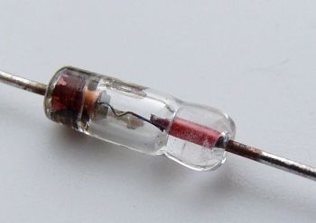
A Diode is that the simplest two-terminal unilateral semiconductor unit. It permits current to flow solely in one direction and blocks the present that flows within the wrong way. the 2 terminals of the diode area unit referred to as as anode and cathode.
The characteristics of a diode closely match to it of a switch. a perfect switch once open doesn't conduct current in either directions and in closed state conducts in each directions.
Ideally, in one direction that's indicated by the arrow head diode should behave short circuited and in alternative one that opposite to it of the direction of arrow head should be open circuited. By ideal characteristics, the diodes is meant to satisfy these options on paper however don't seem to be achieved much. therefore the sensible diode characteristicsare solely near that of the required.
How Diodes work?
The diode operates once a voltage signal is applied across its terminals. the appliance of a DC voltage to create the diode operate in a very circuit is named as ‘Biasing’. As already mentioned higher than the diode resembles to it of a 1 approach switch therefore it will either be in a very state of physical phenomenon or in a very state of non physical phenomenon. The ‘ON’ state of a diode is achieved by ‘Forward biasing’ which implies that positive or higher potential is applied to the anode and negative or lower potential is applied at the cathode of the diode. In alternative words, the ‘ON’ state of diode has the applied current within the same direction of the arrow head. The ‘OFF’ state of a diode is achieved by ‘Reverse biasing’ which implies that positive or higher potential is applied to the cathode and negative or lower potential is applied at the anode of the diode. In alternative words, the ‘OFF’ state of diode has the applied current within the wrong way of the arrow head.
During ‘ON’ state, the sensible diode offers a resistance referred to as because the ‘Forward resistance’. The diode needs a forward bias voltage to modify to the ‘ON’ condition that is named Cut-in-voltage. The diode starts conducting in reverse biased mode once the reverse bias voltage exceeds its limit that is named because the Breakdown voltage. The diode remains in ‘OFF’ state once no voltage is applied across it.
A simple p-n juction diode is fancied by doping p and n kind layers on a semiconducting material or Ge wafer. The Ge and semiconducting material materials area unit prefered for diode fabrication because:
• they're offered in high purity.
• Slight doping like one atom per 10 million atoms of a desired impurity will amendment the conduction to a substantial level.
• The properties of those materials amendment on applying heat and lightweight and thence it's necessary within the devlopment of warmth and lightweight sensetive devices.
Types of Diodes:
The other variant of diodes have completely different construction, characteristics and applications. the various sorts of diodes are:
• tiny signal or tiny current diode - These diodes assumes that the operative purpose isn't affected as a result of the signal is little.
• giant signal diodes - The operative purpose in these diodes get affected because the signal is giant.
• Zener diodes - This diode runs in reverse bias condition once the voltage reaches the breakdown purpose. A stable voltage are often achieved by inserting a resistance across it to liimit the present. This diode is employed to {supply|to produce} reference voltage in power supply circuits.
• lightweight emitting diodes (LED) - this is often the foremost standard reasonably diode. once it works within the forward bias condition, the present flows through the junction to supply the sunshine.
• Photodiodes - The electrons and holes area unit generated as lightweight strikes across the contact inflicting the present to flow. Theses diodes will work as photodetector and area unit accustomed generate electricity.
• Constant current diodes - This diode keeps the present constant even once the voltage applied keeps dynamical. It consists of JFET (junction – field result transistor) with the supply shorted to the gate so as to perform sort of a 2 - terminal current electrical circuit or current supply.
• Schottky diode - These diodes area unit utilized in RF applications and clamping circuits. This diode has lower forward dip as against the semiconducting material PN junction diodes.
• William Bradford Shockley diode - this is often a four layer diode that is additionally called PNPN diode. This didoe is analogous to thyristor wherever the gate is disconnected.
• Step recovery diodes - This semiconductor unit has the power to come up with short pulses and thence it's utilized in microwave applications as a generator.
• Tunnel diodes - This diode is heavily doped within the forward bias condition that features a negative resistance at very low voltage and a brief circuit within the negative bias direction. This diode is beneficial as a microwave ampilifer and in oscillators.
• Varactor diodes - This diode works in reverse bias condition and restricts the flow of current thorugh the junction. reckoning on the number of biasing, the breadth of the depletion region keeps varied. This diode includes of 2 plates of a capacitance with the depletion region amidst them. The variation in capacitance depends upon the depletion region and this will varied by sterilisation the reverse bias on the diode.
• PIN diodes - This diode has intrinsic semiconductor sandwiched between P- kind and N- kind region. Doping doesn't occur during this sort of diode and thereby the intrinsic semiconductor will increase the breadth of the depletion region. they're used as ohtodiodes and frequence switches.
• optical device diode - This diode produces optical device sort of lightweight and area unit overpriced as compared to LED. they're wide utilized in CD and optical disk drives.
• Transient voltage supression diodes - This diode is employed to shield the natural philosophy that area unit sensitive against voltage spikes.
• Gold doped diodes - These diodes use gold because the dopant and may operate at signal frequencies though the forward dip will increase.
• Super barrier diodes - These are referred to as because the rectifier diodes. This diodes have the property of low reverse outflow current as that of traditional contact diode and low forward dip as that of Schottky diode with surge handling ability.
• purpose contact diodes - the development of this diode is easier and area unit utilized in analog applications and as a detector in radio receivers. This diode is made of n – kind semiconductor and few conducting metals placed to be in reality with the semiconductor. Some metals move from towards the semiconductor to make tiny region of p- tpye semiconductor close to the contact.
• Peltier diodes - This diode is employed as engine and detector for thermoelectrical cooling.
• Gunn diode - This diode is formed of materials like GaAs or InP that exhibit a negative differential resistance region.
• Crystal diode - These area unit a kind of purpose contact diodes that are referred to as as Cat’s whisker diode. This didoe includes of a skinny sharpened metal wire that is ironed against the conductive crystal. The metal wire is that the anode and also the semconducting crystal is that the cathode. These diodes area unit obsolete.
• Avalanche diode - This diode conducts in reverse bias condition wherever the reverse bias volage applied across the contact creates a wave of ionization resulting in the flow of huge current. These didoes area unit designed to breakdown at specific reverse voltage so as to avoid any harm.
• semiconducting material controlled rectifier - because the name implies this diode are often controlled or triggered to the ON condition as a result of the appliance of tiny voltage. They belong to the family of Thyristors and is employed in varied fields of DC control, generator field regulation, lighting system management and variable frequency drive . this is often 3 terminal device with anode, cathode and third controled lead logic gate.
• Vaccum diodes - This diode is 2 conductor electronic device which might tolerate high inverse voltages.
Generic diodes (Small signal and huge signal):
A contact diode is that the simplest semiconductor unit. it's a two-terminal, bipolar, unilateral rectifying device that conducts solely in one direction. The generic diodes area unit utilized in the subsequent fields:
• Rectification in power offer circuits
• Extraction of modulation from radio signals in a very wireless and in protection circuits wherever giant transient currents could seem on low current transistors or ICs in interfacing with relays or alternative high power devices.
• utilized in series with power inputs to electronic circuits wherever only 1 of negative or positive polarity voltage is desired.
Construction:
A simple p-n diode could be a junction wherever p-type and n-type layers area unit doped on a semiconducting material or Ge wafer. A semiconductor is made by doping of power or acceptor impurity atoms on a pure semiconducting material or Ge thereby having AN excess concentration of holes. AN semiconductor unit is made by doping of power or donor impurity atoms on a pure semiconducting material or Ge thereby having AN excess concentration of electrons. So, holes area unit the bulk charge carriers in a very p-type region whereas electrons within the n-type region. Electron-holes pairs area unit thermally generated in each sorts that represent the minority charge carriers. it's exceptional that a p-type material isn't charged in spite of getting excessive holes whereas AN n-type material isn't charged in spite of excessive electrons. this is often as a result of in a very p-type material beside holes, the anions area unit generated and also the total range of protons and electrons still stay constant. this is often equally determined for the n-type material.
The junction of a p-type and n-type doping on semiconducting material or Ge wafer produces atiny low region of the order of micrometers that is depleted from the free charge carriers. This region is made as a result of diffusion of holes from a p-type ANd electrons from an n-type material referred to as because the depletion region or area charge region or transition region. The p-type region to the left of the depletion region has acceptor negative particle layer and to the proper area unit donor positive particle layer that induces an electrical flux or potential across the junction. The charge concentration is positive on left of the junction and negative on the proper of the junction. This potential barrier stops the holes to migrate into n-type region and electrons to migrate into p-type region because the potential rises for holes and electrons can enable migrating in to n-type and p-type regions. The charge carrier regions round the depletion regions are referred to as because the uncovered regions.
It is conjointly necessary that the minority charge currents i.e. negatron current in p-type region and hole current in n-type region decreases exponentially across the diode length. The minority current is as a result of negatron hole pairs generated thermally and dependent upon temperature. These currents area unit therefore tiny in magnitude within the order of microamperes. but in physical phenomenon state, the present through the diode crystal remains stable. the full current could be a add of minority and majority charge currents as a result of bipolar nature of the diode. the bulk charge currents is hole current in p-type and negatron current in n-type area unit reduced as they migrate close to junction due recombination. The minority currents is negatron current in p-type ANd hole current in n-type area unit most close to junction and reduces as they migrate off from the junction as an exponential. the bulk charge currents in their regions once crossing the junction area unit the diffusion currents whereas before junction area unit drift currents.
Concept of resistance unit contacts – additionally to PN junction diode, there's a 2 metal semiconductor junctions originating from the leads so as to attach the device. it's assumed that the resistance of those metal semiconductor contacts stay constant despite of the magnitude and direction of current. throughout the diode operation, the applied voltage is entirely effective for increasing or decreasing the potential barrier height of the PN junction.
Principle and Operation:
The doable configurations for a diode are:
1. Open circuited
2. Short circuited
3. Forward biased
4. Reverse biased
1. Open circuited: In open circuited condition, the present that flows through the diode is zero (I = 0). The potential barrier at the PN junction remains constant as created within the diode fabrication.
2. Short circuited: briefly circuited condition, the add voltage within the loop should be zero. therefore it's assumed, that the potential barrier at the PN junction is salaried by the potential drops at the metal semiconductor junctions. The holes provided by the n-region should be driven to the p region that is physically not possible. The similar discussion applies to the negatron current within the n-region.
3. Forward bias: In forward bias condition, higher or positive potential is applied at the anode and negative or lower potential is applied at the cathode of a diode. The positive potential at anode repels the holes in p-region towards n-region whereas negative potential at the cathode repels electrons in n-region towards p-region. Thus, the peak of the potential barrier reduces. The depletion region disappears once the applied voltage equals to the potential barrier and an oversized current flows through the diode. The voltage needed to drive the diode into a state of physical phenomenon is named because the ‘Cut in/Offset/Threshold/Firing voltage’. the present is of sizable magnitude because it is dominantly accepted by the bulk charge currents that's the outlet current within the p-region and also the negatron current within the n-region. the present that flows from anode to cathode is restricted by the crystal bulk resistance, recombination of charges and also the resistance unit contact resistances at the 2 metal semiconductor junctions. the present is restricted to milli Amperes order.
4. Reverse Bias: In reverse bias condition, the upper or positive potential is applied at the cathode and negative or lower potential is applied at the anode. The negative potential at anode attracts the holes in p-region that area unit off from the n-region whereas positive potential at the cathode attracts electrons in n-region that area unit off from the p-region. The applied voltage will increase the peak of the potential barrier. the present flows dominantly as a result of the minority charge currents that's the negatron current in p-region and also the hole current in n-region. therefore a continuing current of negligible magnitude flows within the reverse direction that is named because the ‘Reverse saturation current’. much, the diode remains in a very state of non – physical phenomenon. The reverse saturation current is of the order of microamperes in a very Ge diode or nanoamperes in a very semiconducting material diode If the reverse voltage exceeds the limit of ‘breakdown/Zener/Peak inverse/Peak reverse voltage’, the potential breakdown that happens results in an oversized reverse current.
Datasheet Analysis:
The datasheets of the diodes offers valuable stuff regarding their varied parameters such as:
• Peak inverse voltage,
• Reverse saturation currents at mere reverse voltages, most forward current.
• Capacitance levels,rse recovery time.
• Storage and operative temperatures.
• Peak repetitive forward current.
• Peak forward surge current.
• Average surge current and lots of additional.
The graphs to represent the voltage current characteristics and temperature dependences are provided.
Rectifying Diodes in Market:
• Diodes selected from IN4001 to IN4007 area unit offered with most forward voltage of one.1 V and oneA being the most rectifying current. the most reverse current area unit five uA and PIV (Peak Inverse voltage) varies from 50V to 1000V.
• Another series of diodes is IN5400 to IN5408 with most forward voltage of one.2 V and 3A being the most rectifying current. the most reverse current area unit five uA and PIV (Peak Inverse voltage) varies from 50V to 1000V.
Testing of a Diode:
A diode are often open circuited or short circuited once broken. It are often tested employing a multimeter by following the steps given below:
1. Insert the probes into the specified sockets: The digital multimeter can have many sockets for the take a look at probes. Insert these probes and check if they're already within the correct sockets. Typically, these area unit labeled COM for common and also the others for current or voltage. this is often commonly combined with the voltage measure socket.
2. activate the multimeter and choose the most resistance vary.
3. Check resistance in forward and reverse direction. Place the red probe on diode anode and black probe on the cathode to live the forward resistance. Place the red probe on diode cathode and black probe on anode to live the backward resistance. The forward resistance should be terribly tiny in few ohms whereas backward resistance should be terribly high within the vary of mega ohms. If forward resistance is incredibly high the diode is open circuited and if backward resistance is incredibly tiny diode are short circuited.
4. in our own way is to pick out diode on the multimeter. Place the red probe on diode anode and black probe on the cathode and of the multimeter beeps then it indicates a brief circuit otherwise it's open. Place the red probe on diode cathode ANd black probe on the anode and if the multimeter doesn't beep then it indicates an electric circuit otherwise if it beeps the diode is brief.
5. shut down the multimeter: Once the resistance measure has been created, the multimeter are often turned off to preserve the batteries. it's conjointly informed flip the perform switch to a high voltage vary. during this approach, if the multimeter is employed once more for one more sort of reading then no harm are caused if it's unknowingly used while not choosing the right vary and performance.
Conclusion:
Diodes area unit utilized in varied applications like rectification, clipper, clamper, voltage number, comparator, sampling gates and filters.
1. Rectification – The rectification means that changing AC voltage into DC voltage. The common rectification circuits area unit [*fr1] wave rectifier (HWR), full wave rectifier (FWR) and bridge rectifier.
Half wave rectifier: This circuit rectifies either positive or negative pulse of the input AC.
Full wave rectifier: This circuit converts the complete AC signal into DC.
Bridge rectifier: This circuit converts the complete AC signal into DC.
2. Clipper- Diode are often accustomed clip off some portion of pulse while not distorting the remaining a part of the wave shape.
3. Clamper – A clamping circuit restricts the voltage levels to exceed a limit by shifting the DC level. the height to peak isn't suffering from clamping. Diodes with resistors and capacitors area unit accustomed build clamping circuits. generally freelance DC sources are often accustomed give extra shift...